Specification
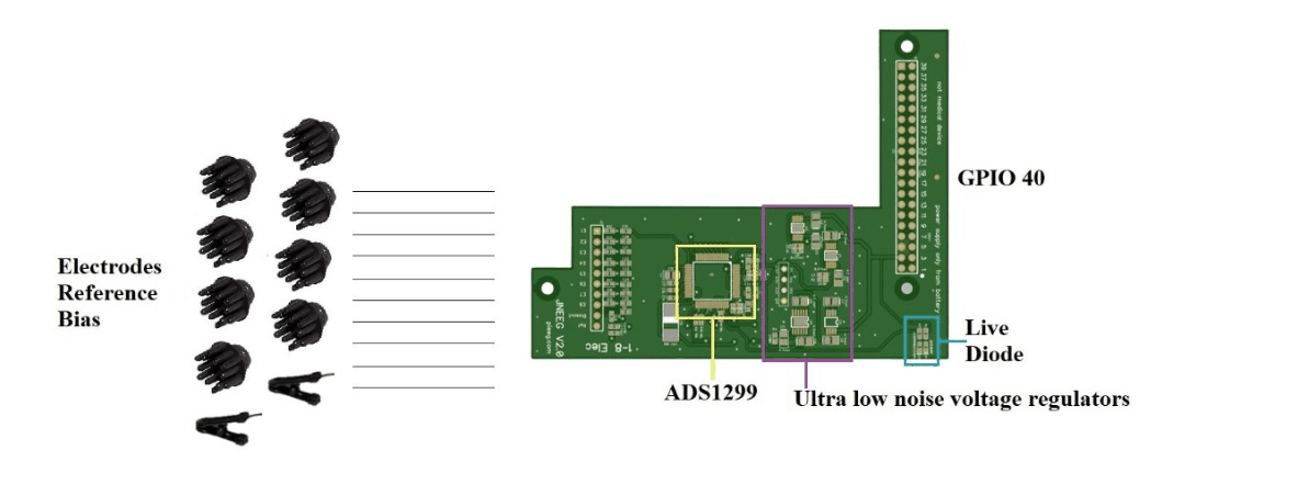
Hardware
| Channels | 8 single-ended biosignal inputs |
| Extra inputs | Reference (shared by all channels) and bias |
| Analog front end | Texas Instruments ADS1299 |
| Resolution | 24-bit, delta-sigma, all channels sampled at the same moment |
| Sample rate | 250 SPS as set by PiEEG software (the ADS1299 supports 250 SPS to 16 kSPS) |
| Gain | 1 as set by PiEEG software (the ADS1299 supports 1, 2, 4, 6, 8, 12, 24) |
| Reference voltage | 4.5 V internal |
| Power regulation | Ultra-low-noise voltage regulators on the board |
| Status LED | On when the board is powered |
| Signals | EEG, EMG, ECG |
| Electrodes | Dry or wet Ag/AgCl, 2.54 mm header |
| Host | NVIDIA Jetson Nano Developer Kit, 40-pin header |
| Interface | SPI (/dev/spidev0.0) and DRDY on header pin 7 |
| Power | 5 V via the Jetson Nano, from a power bank only |
| Isolation | None. Battery operation is required. |
Software support
| Software | Setting |
|---|---|
| PiEEG Server | --device jneeg (applies the jetson-nano profile) |
| Python scripts (opens in a new tab) | 1.Graph_real_time.py, 2.Save_data.py |
Pins and SPI
| Header pin | Signal |
|---|---|
| 19 | SPI MOSI |
| 21 | SPI MISO |
| 23 | SPI SCK |
| 24 | SPI CS0 |
| 7 | DRDY (active low) |
| Setting | Value |
|---|---|
| Device | /dev/spidev0.0 (spi1 in jetson-io) |
| Mode | 1 (CPOL 0, CPHA 1) |
| Bit order | MSB first |
| Clock | 600 kHz |
| DRDY in PiEEG Server | /dev/gpiochip0, line 216 |
| DRDY in the Python scripts | Jetson.GPIO, board pin 7 |
Data frame
Each time DRDY goes low, read 27 bytes:
| Bytes | Content |
|---|---|
| 1–3 | ADS1299 status word |
| 4–6 | Channel 1 |
| … | … |
| 25–27 | Channel 8 |
Each channel is a 24-bit, big-endian, two's-complement value.
Converting to microvolts
The conversion used by the PiEEG scripts and PiEEG Server:
raw = (b[0] << 16) | (b[1] << 8) | b[2]
if raw & 0x800000:
    raw -= 16777214
uV = raw * 4.5 / 16777215 * 1_000_000    # about 0.268 µV per count
Default register settings
Start-up: WAKEUP (0x02), STOP (0x0A), RESET (0x06), SDATAC (0x11), write the registers below, then RDATAC (0x10) and START (0x08). Write a register with [0x40 | address, 0x00, value].
| Address | Register | Value | Meaning |
|---|---|---|---|
0x01 | CONFIG1 | 0x96 | 250 SPS |
0x02 | CONFIG2 | 0xD4 | Internal test-signal settings (not used in normal mode) |
0x03 | CONFIG3 | 0xFF | Internal reference buffer on, internal bias reference, bias buffer on |
0x04 | LOFF | 0x00 | Lead-off detection off |
0x05–0x0C | CH1SET–CH8SET | 0x00 | Normal electrode input, gain 1 |
0x0D–0x11 | BIAS_SENS, LOFF_SENS, LOFF_FLIP | 0x00 | |
0x14 | GPIO | 0x80 | |
0x15 | MISC1 | 0x20 | Reference electrode shared by all channels (SRB1) |
0x17 | CONFIG4 | 0x00 | Continuous conversion |
Noise self-test: set every CHnSET to 0x01 (input shorted). The signal should stay within a few µV. See Noise elimination.